

Effective Capacitance of Inductive Interconnects
Abstract—Interconnect resistance and inductance
shield part of
the load capacitance, resulting in a faster voltage transition at the
output of the driver. Ignoring this shielding effect may induce significant
error when estimating short-circuit power. In order to capture
this shielding effect, an effective capacitance of a distributed
 load is presented for accurately estimating
the short-circuit
load is presented for accurately estimating
the short-circuit
power. The proposed method has been verified with Cadence
Spectre simulations. The average error of the short-circuit power
obtained with the effective capacitance is less than 7% for the example
circuits as compared with an  model. This
effective
model. This
effective
capacitance can be used in look-up tables or in empirical -factor
expressions to estimate short-circuit power.
Index Terms—Interconnect,
, shielding effect, short-circuit
power.
I. INTRODUCTION
SINCE power has become an important design criterion in
integrated circuits, accurate and efficient power estimation
is required in the circuit design process. As compared with dynamic
power which is well characterized, short-circuit power
is more difficult to model due to the complicated transient behavior
of the short-circuit current [1].
The short-circuit power dissipation in a gate is primarily
determined by three factors: input signal transition time, load
capacitance, and size of the transistors in the gate. In [2],
Veendrick developed a closed-form expression for short-circuit
power dissipation in an unloaded CMOS inverter. More
accurate device models have recently been adopted to analyze
short-circuit power [3], [4]. It is shown in [4] that short-circuit
power can be as high as 20% of the total active power in high
speed, low voltage circuits. As interconnect coupling becomes
more significant in advanced technologies, the impact of
crosstalk noise on the short-circuit power is analyzed in [5] by
introducing an effective input slew. In these analyses, a lumped
capacitor is assumed as the load. With CMOS technology
scaling, the interconnect resistance can be comparable to the
gate resistance and should be included in the load model. In
[6], a π shaped  model is adopted as the load.
An effective
model is adopted as the load.
An effective
capacitance of the  structure for
short-circuit power
structure for
short-circuit power
estimation is described in [7] and [8] to maintain compatibility
with popular look-up table or -factor based power models.
With increasing on-chip frequencies and longer interconnects,
the interconnect inductance can also no longer be ignored.
As described in [9], the interconnect inductance also exhibits
a shielding effect on the load capacitance, increasing the
short-circuit power dissipated by the driver.
In [10], an effective capacitance of an
load is developed
to accurately estimate short-circuit power. This effective capacitance
model is extended in this paper. The importance of the
inductive shielding effect is identified and the model is further
verified for gates with unaligned multiple inputs. The rest of this
paper is organized as follows. In Section II, a distributed
network is reduced into a π model. From this π model, the effective
capacitance is determined. In Section III, the proposed
effective capacitance model is verified by Cadence Spectre simulations
for gates with single and multiple inputs. Finally, some
conclusions are offered in Section IV.
II. EFFECTIVE CAPACITANCE OF AN INDUCTIVE LOAD
Model order reduction techniques are commonly used to
analyze
the timing and power of interconnects to improve simulation
efficiency. In Section II-A, a π model is generated from
a distributed tree through a typical model
order reduction
method—moment matching. In Section II-B, this π model
is further reduced into an effective capacitance by matching the
average charging/discharging current.
A. π Model Representation of
Interconnects
In [11], an  network is
reduced to an
network is
reduced to an  model by
matching the first three moments  of the
admittance
of the
admittance
at the driving point. Similarly, an  network
can be reduced
network
can be reduced
to an  model by matching the first four
moments,
model by matching the first four
moments,
as shown in Fig. 1. This reduction, however, can be unrealizable
(the value of the circuit element is not positive real). In order to
obtain a realizable  model, a coefficient
 is introduced
in [12], which is the third order admittance moment without considering
the inductance. By matching  , the π
model parameters can be obtained as [12]
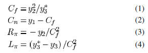
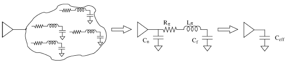
Fig. 1. Reduction of an RLC interconnect network.
where  and
and
 denote the near end and far end capacitance,
respectively.
The input admittance of a distributed
 interconnect with
a load admittance  is [13]
where  and
and
 are the total resistance, capacitance, and
inductance of the interconnect,
are the total resistance, capacitance, and
inductance of the interconnect,
respectively. By expanding  into a Taylor
series
into a Taylor
series
of s around zero, the moments at the input of the
 interconnect
can be obtained as
The input admittance moments of a distributed
tree can
be determined by recursively applying (6)–(9). From these moments
and (1)–(4), the corresponding π structure can be obtained.
B. Effective Capacitance for Short-Circuit Power
Although a π model is highly accurate, four coefficients
are
required in this model, making it incompatible with k-factor
expressions or look-up table based power models. An effective
capacitance greatly simplifies the model with little penalty in
accuracy, as shown in Fig. 1.
The shielding effect of the interconnect resistance is
well
known and the effective capacitance of  interconnects has
been developed for estimating delay and short-circuit power in
[7], [14]. The interconnect inductance however also exhibits a
shielding effect [9]. This inductive shielding effect is illustrated
with an example, as shown in Fig. 2. In Fig. 2, a distributed

tree is driven by a  CMOS inverter. Since the
shielding
CMOS inverter. Since the
shielding
effect of the interconnect is only significant in interconnect loads
with a high impedance which are generally driven by large gates,
a large inverter is considered with transistor sizes,

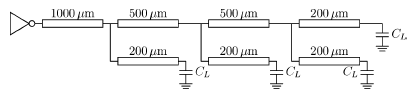
Fig. 2. Example of a distributed RLC tree.
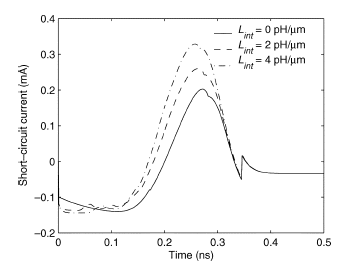
Fig. 3. Effect of inductance on short-circuit current.
 ns.
ns.
and  The impedance
parameters of the interconnect
The impedance
parameters of the interconnect
are 
These impedance values are extracted from a typical top layer
wire structure in a CMOS technology. The
wire width
is  and wire thickness is
 The load capacitance is
 . The short-circuit current in the inverter
is illustrated
. The short-circuit current in the inverter
is illustrated
in Fig. 3 for different values of interconnect inductance.
When the interconnect inductance becomes larger, a greater far
end capacitance is shielded. Less effective capacitance is therefore
seen at the inverter output, permitting the output voltage to
change faster at the beginning of the signal transition, thereby
producing a larger short-circuit current. The currents are measured
at the source of the pMOS transistor with a rising edge
input as shown in Fig. 4. The discontinuity of the waveform
is due to the discontinuity of the transistor capacitance model
used in the simulation. Strictly speaking, the currents shown in
Fig. 3 include two non-short-circuit current components. The
first component is the current flowing through the capacitance
 , as shown in Fig. 4. This component can be
determined as
, as shown in Fig. 4. This component can be
determined as
 and is independent of the load. The second
component is the current  flowing from the
output to
flowing from the
output to  due
due
to the overshoot at the output at the beginning of the signal transition.
returns a small amount of charge stored in
the output
node back to , slightly reducing the dynamic
power.
In [14], the output waveform of a CMOS gate is
approximated
by a quadratic function followed by a linear function. In this
paper, the output waveform of a gate is modeled as a quadratic
function during the input transition. Assuming the output waveform
is  for a rising edge, the current drawn from
the
for a rising edge, the current drawn from
the
gate by an  structure is
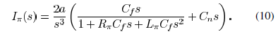
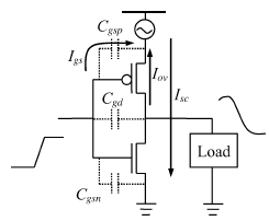
Fig. 4. Current components in a CMOS inverter.
Applying an inverse Laplace transformation to (10), the
current
in the time domain is

where
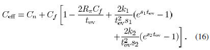
The current drawn from the gate by an effective capacitance is
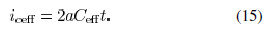
Equating the average of  and
and  during a period from 0 to
an evaluation time  , can be obtained as
Similarly,  for an
 structure is
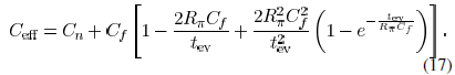
As expected, is
between 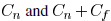 . From (16),
is a function of  as shown in Fig. 5. The π
model parameters
as shown in Fig. 5. The π
model parameters
are obtained from the tree structure as shown in Fig. 2 with an
inductance per unit length  . With increasing
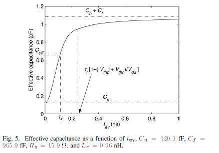
 increases from
 and approaches
 . In [14],
is the time when the driver output achieves 50% of
 , which
is the objective and is not known a priori. Several iterations are
therefore required to determine  . In [7],
 is determined as
the end point of the short-circuit period. Since the short-circuit
current exists when the input is between  the
the
appropriate evaluation time  is in the range
from 0 to
is in the range
from 0 to 
 . Note that
 corresponds to
the time when the input reaches  for a rising
edge
for a rising
edge 
 for a falling edge). As shown in Fig. 5, for
the time period
for a falling edge). As shown in Fig. 5, for
the time period
 , the effective capacitance is overestimated
and the
, the effective capacitance is overestimated
and the
short-circuit current is underestimated. For the period

 , the effective capacitance
is underestimated and the short-circuit current is overestimated.
By properly adjusting  , the estimation error
of the short-circuit
, the estimation error
of the short-circuit
current in different time regions can be canceled. By comparing
Spectre simulations, a fitting parameter is adopted to determine
The short-circuit current waveforms in an inverter with
different
load models are compared in Fig. 6. For this inverter,
 . As shown in Fig. 6, the π
model can accurately characterize a tree structure. The waveform
obtained with a π model is indistinguishable from the
waveform with the original  tree (shown in
Fig. 2). Using
tree (shown in
Fig. 2). Using
the total capacitance 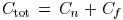 as the load, however,
significantly underestimates the short-circuit current. As previously
mentioned, the short-circuit current with the effective capacitance
is first underestimated and then overestimated. No iterations
are required to determine  . Since an
 model
model
is commonly required in timing analysis, the additional computational
expense required to determine is small. Note
that
unlike for estimating the delay [14],
for short-circuit
power estimation is independent of the transistor size.
III. MODEL VERIFICATION
The proposed effective capacitance model is verified with
gates with a single input (inverter), multiple inputs, and unaligned
multiple inputs in Section III-A–C, respectively.
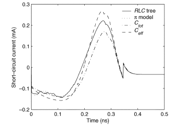
Fig. 6. Short-circuit current with different output loads.
A. Gate With Single Input
For the example circuit shown in Fig. 2, the short-circuit
energy
dissipated over a full signal transition with different loads is
compared in Fig. 7. As shown in Fig. 7, the total capacitance always
underestimates the short-circuit energy as compared with
a distributed  tree. For example, the error
for
tree. For example, the error
for  ns is
ns is
28.1%. More accurate estimations can be obtained with

(only considering the resistive shielding effect) and
 (considering
both resistive and inductive shielding effects).
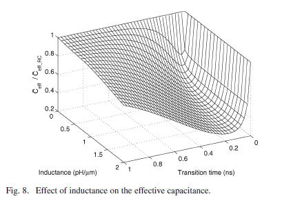
The inductive shielding effect is most important for this
example
in the range from  . The inductive
shielding effect can be evaluated by the ratio of

to  . In Fig. 8, this ratio is plotted with
different input
. In Fig. 8, this ratio is plotted with
different input
transition times and wire inductances for the example circuit
shown in Fig. 2. As shown in Fig. 8,  decreases with increasing
interconnect inductance. The ratio of 
can be smaller than 0.3. When  approaches
zero, the driver
approaches
zero, the driver
only sees the near-end capacitance, both  approach
 , and the ratio
 approaches one. When
 is sufficiently large, the driver has
sufficient time to charge
is sufficiently large, the driver has
sufficient time to charge
and discharge the far end capacitance, both 
approach  , and the ratio also approaches one.
Since the dynamic power is usually determined as
 (where α is the switching factor), the
reduction
(where α is the switching factor), the
reduction
in dynamic power  due to
 is considered part of the
short-circuit power such that the summation of the two power
components (dynamic and short-circuit) can represent the
total transient power. With fast inputs,
 can dominate the
short-circuit power, producing a negative short-circuit power,
as shown in Fig. 7. Since cannot be
characterized by  ,
,
the error of the power estimation is greater for fast inputs. With
very slow inputs, although the output voltage waveform deviates
from a quadratic behavior, the proposed method remains
accurate as shown in Fig. 7. In these cases, the shielding effects
are small, and the effective capacitance approaches
 . This
behavior is well captured by (16).
B. Gate With Multiple Inputs
The effective capacitance concept can also be applied to
other
logic gates with multiple inputs, such as NAND and NOR gates.
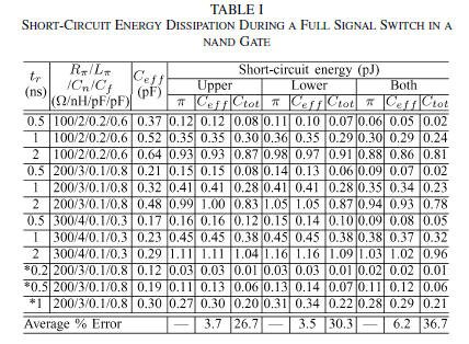
The short-circuit energy consumed by a two input NAND gate
during a full signal transition is listed in Table I for different
input transition times and interconnect loads. The two inputs
of the NAND gate are denoted as the upper input and the lower
input according to the relative position of the input terminal.
Three switching patterns are considered: only the upper input is
switched (the lower input is tied to  ), only
the lower input is
), only
the lower input is
switched, and both of the two inputs are connected and simultaneously
switched. The size of the transistors in the NAND gate
is The rows starting with an
 are obtained with a 45-nm [15] CMOS NAND
gate, and the
are obtained with a 45-nm [15] CMOS NAND
gate, and the
transistor sizes are  . As listed
in Table I, the effective capacitance can accurately capture the
shielding effect of the resistance and inductance in
determining
the short-circuit power. The average error of the short-circuit
power is less than 7% as compared with the π model. The average
error with the total capacitance, however, is more than
26% for these examples. Note that for a 45-nm CMOS technology,
a new fitting parameter can be determined to further improve
the accuracy of the model.
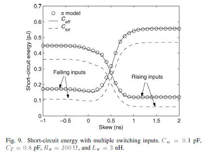
C. Gate With Unaligned Multiple Inputs
For multiple switching inputs with offsets in delay
(non-simultaneous
input signals), an equivalent input signal has been
developed in [16] for estimating the short-circuit power. From
this equivalent input signal, an effective capacitance can be obtained
from (16) and (18). The short-circuit energy dissipated
in a NAND gate is shown in Fig. 9 for different skew between
the two inputs. The transition time of the upper input and lower
input is 1 and 2 ns, respectively. The skew is determined as
 are the starting time of
the transition at the upper input and lower input, respectively.
From Fig. 9, it can be seen that the effective capacitance model
is also valid for multiple switching inputs with delay offsets.
Look-up tables or -factor expressions are commonly used
to model short-circuit power as a function of
 . The
. The
total transient power in a CMOS gate driving an interconnect
network, therefore, can be represented as

where  includes the
total interconnect capacitance and the
includes the
total interconnect capacitance and the
parasitic capacitance of the transistors. If glitches occur at the
output, both dynamic power and short-circuit power depend
upon the transient voltage waveform at the output. Expression
(19) is no longer valid in this case and a more complicated analysis
is required.
IV. CONCLUSIONS
As CMOS technology is scaled, the interconnects not only
dominate the overall circuit delay, but also greatly affect the
power dissipation. The dynamic switching power of a circuit
is directly related to the total interconnect capacitance. Using
the total interconnect capacitance to estimate the short-circuit
power, however, can lead to significant error due to the shielding
effect of the interconnect impedance. In this paper, an effective
capacitance of a distributed  load is
developed to accurately
load is
developed to accurately
estimate the short-circuit power. The average error of the
short-circuit power obtained with  is less
than 7% as compared
is less
than 7% as compared
with an  model. This effective capacitance
can be
model. This effective capacitance
can be
used in look-up tables or in empirical -factor expressions to estimate
short-circuit power as well as in analytic models to simplify
the interconnect analysis process.